I/O Config Register
To enable bi-directional GPIOs and variable Analog gains, an IO config register is implemented within the HV-Expansion Shields electronics. It is based on 74HC595 shift registers and consists of the Data Direction Register (DDR) and an Analog Gain Register.
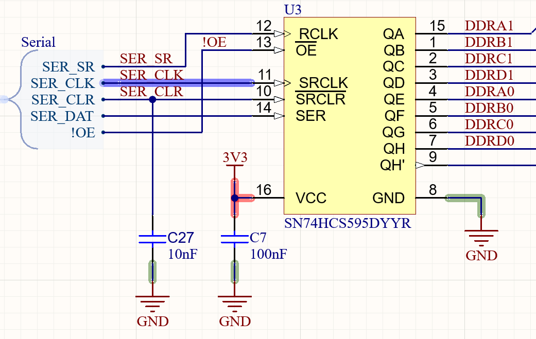
74HC595 as implemented on the HV Shield
Shift register Interface
µC Pin |
shift register function |
shift register pin |
|---|---|---|
PE2 |
Serial clock |
SER_CLK |
PE6 |
Serial data |
SER |
PE3 |
Set register |
RCLK |
PC7 |
!Output Enable |
OE |
Reset |
!clear serial Register |
SRCLR |
In total, the IO Config Register consists of 5 daisy-chained shift registers. Data can be stored, by writing it to the serial in registers of the 595 ICs and then clocking the parallel output registers via a rising edge on RCLK.
Startup
During startup the Outputs of the 74HC595 Registers is undefined. To prevent random activation of the output drivers, !OE is pulled high which configures the shift register’s outputs as High-Impedant. The internal pulldowns of the output drivers then ensure, that all IOs default to a passive state (Input Pins). The analog gains stay undefined this way, which should not cause any issues. Initializing the Registeres after startup should happen as follows:
Ensure, that PC7 (!Output Enable) is initialized as passive, HIGH or in pullup mode.
The mainboard should initialize the registers with 0x0000000000
- Using “set register” this state has to be clocked into the parallel output register.
Now all Outputs are in LOW state.
only now “!Output Enable” can be set to low, enabling the shift register’s output.
See also: https://www.ti.com/lit/ds/symlink/sn54hc595-sp.pdf?ts=1711550377589
Bitmap DDR:
A high state enables the high voltage ouput driver → The IO can be used as an output
A low state disables the high voltage ouput driver → The IO can be used as an input
Bit |
HV-Shield Pins |
|---|---|
0..3 |
5-8 |
4..7 |
1-4 |
8..11 |
13-16 |
12..15 |
9-12 |
16..19 |
21-24 |
20..23 |
17-20 |
24..27 |
29-32 |
28..31 |
25-28 |
Bitmap of the Analog Gain section
Bits |
Gain Bits |
|---|---|
32-39 |
AV0-AV7 |
Using those bits the voltage gains can be configured, as described in: Analog Output