GPIO
The mainboard IOs are 3.3 V or 5V tolerant. the 5V tolerant IOs show an extra “x“ as an indicator on the PCB silkscreen.
I/O Pinout
The GPIOs can be accessed via an Arduino-compatible pin header arrangement and an additional (non-Arduino-compatible) 32-pin header.
Arduino Header
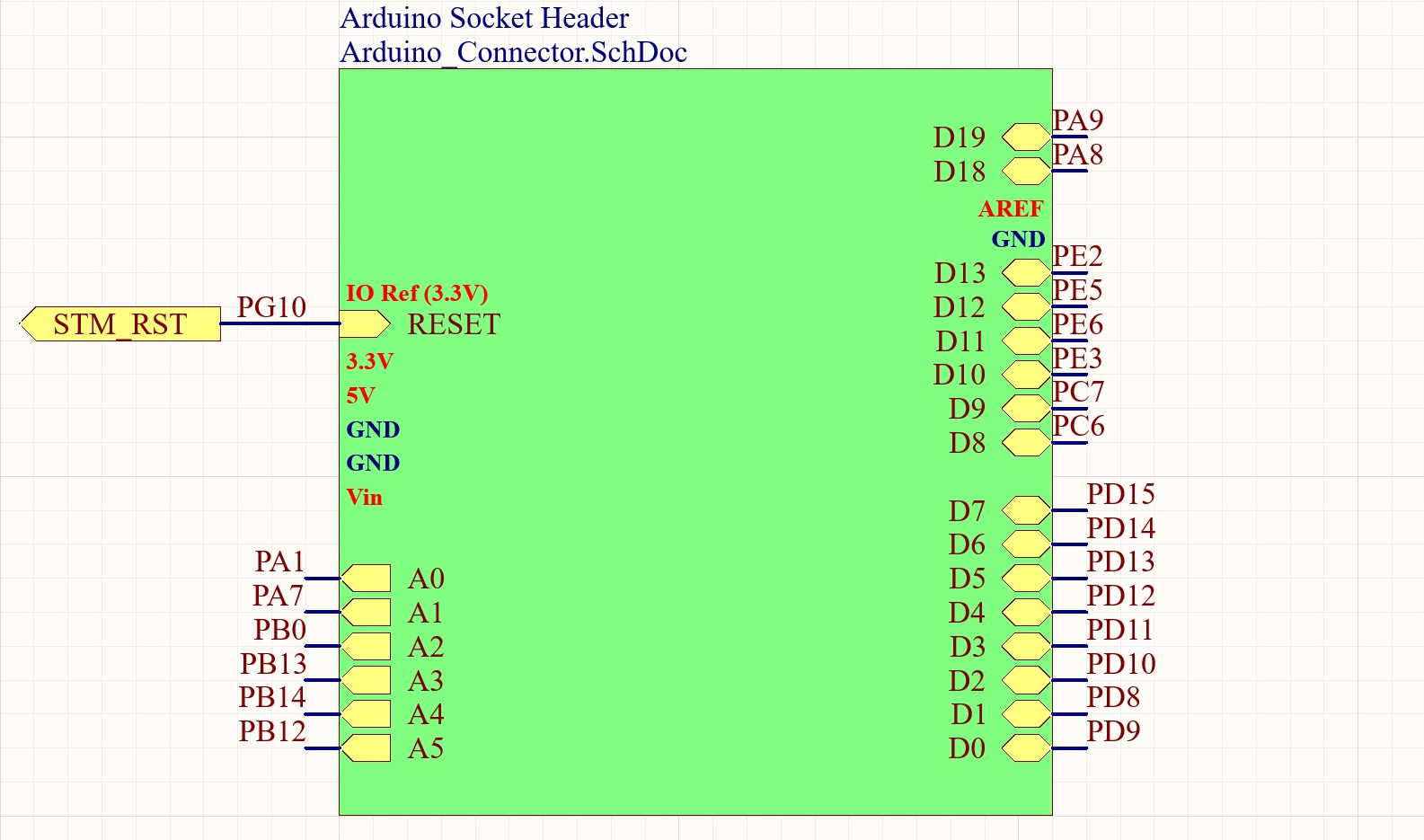
Arduino Pinout starting from rev 0.2
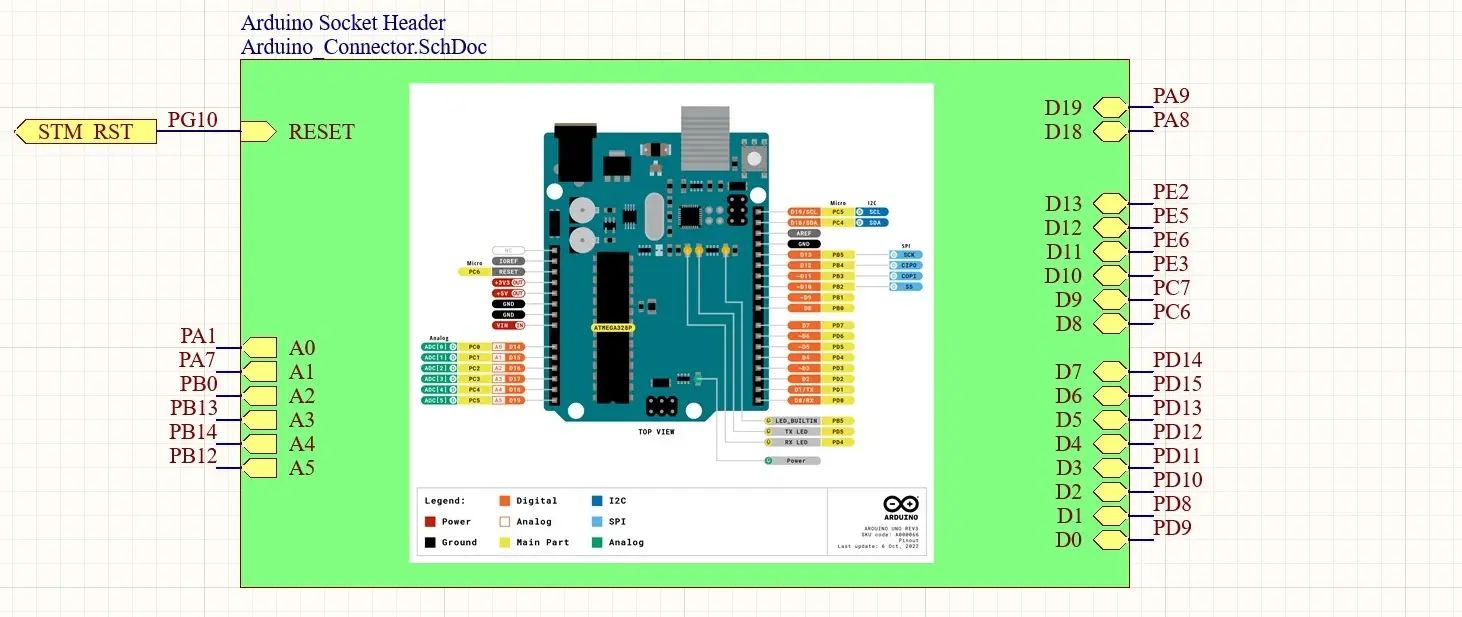
Arduino Pinout up to rev 0.1
32-Pin Header
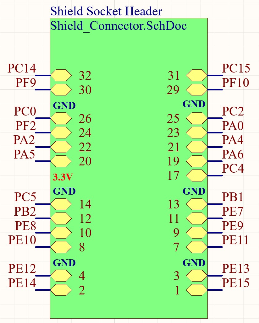
32-Pin connector starting from rev 0.2
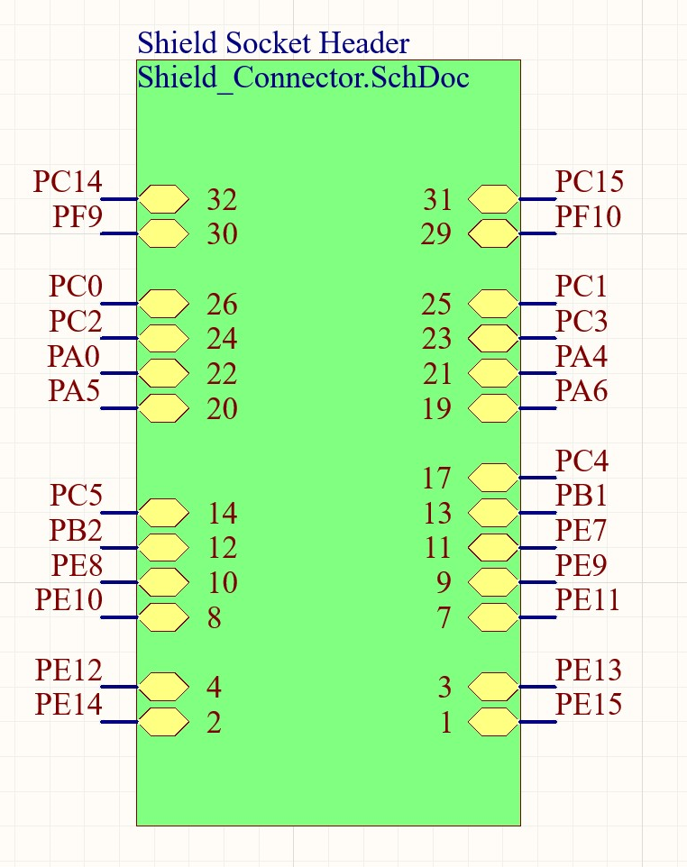
32-Pin connector up to rev 0.1
I/O protection
ARDEP rev1 relied on a combination of snapback diodes and polyfuses as input protection. Due to the poor availability of the snapback diodes and the lack of differentiation between 3.3V and 5V GPIOs, a new approach based on actively clamped protection rails was implemented from ARDEP 2.0 onwards.
All ARDEP GPIOs are equipped with the same polyfuses as revision 1 and an ESD clamping diode.
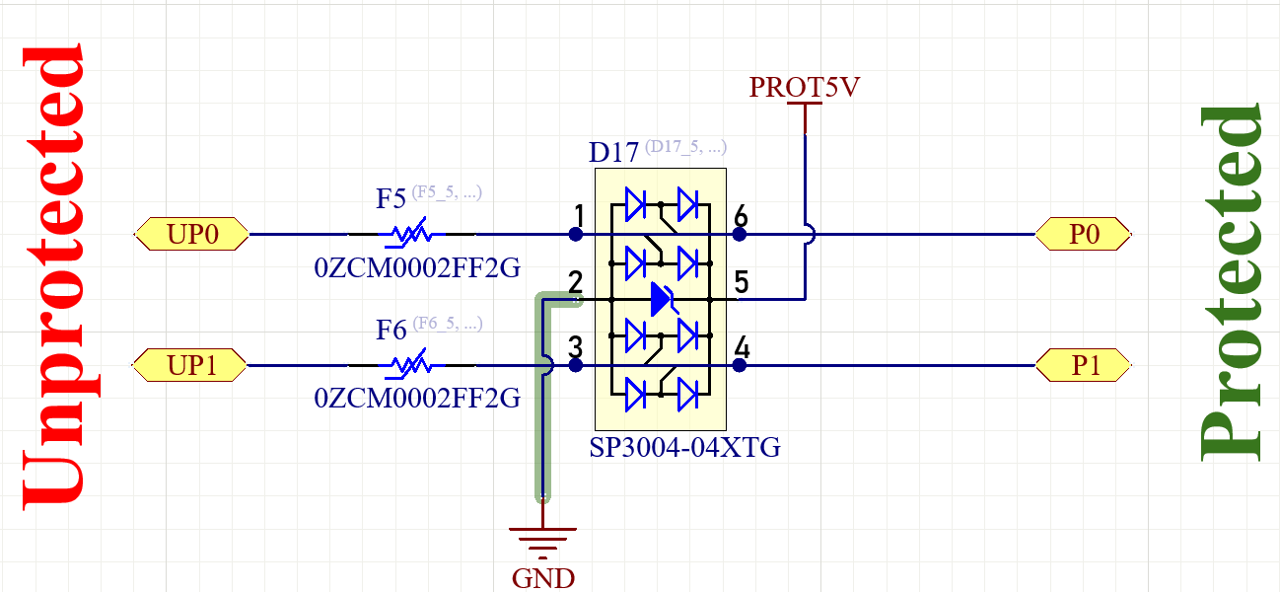
Fundamental input protection circuit (for 5V GPIOs)
Instead of clamping an overvoltage to the LDO-regulated 3.3V or 5V rail of the ARDEP mainboard, a separate rail with TLA431 shunt references set to the respective voltage is used. In contrast to the main 3.3V and 5V supply rails, these protection rails can sink a constant current of 100mA and are therefore suitable for suppressing continuous overvoltage at the board’s GPIOs.

Protection rails clamp circuit
D18 and D19 are placed to prevent cross currents and to ensure a stable supply voltage of the ARDEP mainboard, while still supplying the shunt references with their standby quiescent current.
This also results in the clamp rails being slightly below the supply voltages. This can cause a reduced reverse bias of the ESD diodes at a full swing input and therefore slightly increased capacitive loading of the applied signal.
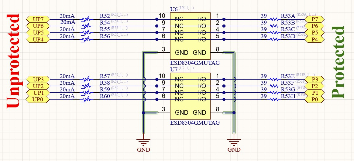
All GPIOs are Protected from ESD and a catastrophic High Voltage event.
Every IO is equipped with the protection circuit illustrated in the figure below. It consists of a self-resettable 20mA poly fuse, a snap-back ESD diode, and an additional series resistor.
The snap-back diode is a special kind of ESD Diode, which triggers, once a certain threshold voltage (in this case ~6V) is reached. It then proceeds to clamp the input voltage to a rather low level of ~1.2V. This is crucial in case of a continuous overvoltage event (e.g. accidental connection of 12V or 24V). The low clamping voltage limits the dissipated power within the ESD diode which protects the diode and leads to a faster triggering of the polyfuse.
In case of a continuous overvoltage of below ~8V at the connector, it cannot be guaranteed, that the snapback diode triggers. Even though it will start to clamp the voltage, an out-of-spec overvoltage may occur at the µC IO Pin and the IC’s internal ESD Protection will engage. To mitigate potential damage to the µC the 39 Ohm series resistor will limit the current into the µC’s ESD protection circuit.
This rather robust protection circuit results in a GPIO output resistance of up to 109 Ohm. This will be the main bandwidth limiting factor of the digital IOs and could be adjusted in a tradeoff between IO-speed and IO-robustness.
TODO CAPTION
UART
The two UART channels are treated like all the other GPIOs. They are routed to a separate spring contact terminal which can therefore be used for UART, or four general-purpose IOs.
Analog I/O
Analog IOs are not separately treated on the mainboard. Instead, all µC GPIOs with analog functions can be software-defined and used accordingly.